Chip on Submount (CoS) bonding testing solutions play a critical role in ensuring the reliability, performance, and longevity of advanced semiconductor and optoelectronic devices. As chip packaging technologies evolve to support higher power densities, miniaturization, and enhanced thermal performance, CoS bonding has emerged as a preferred approach, particularly in laser diodes, LEDs, photonics, and power electronics. Testing solutions designed for this process focus on verifying bond integrity, electrical performance, and mechanical stability to meet stringent industry requirements.
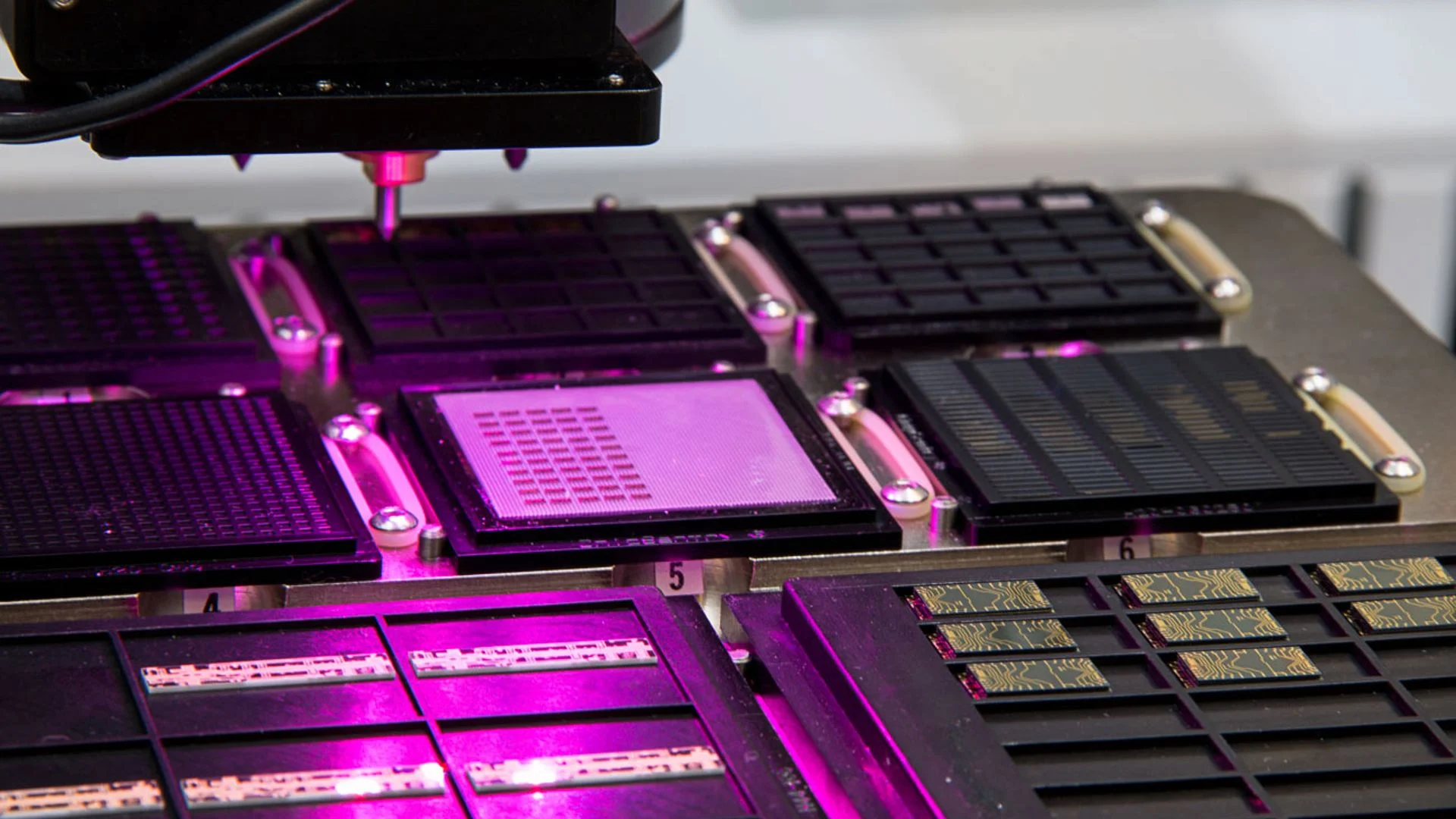
The Chip on Submount bonding process involves attaching a semiconductor die directly onto a submount material, such as ceramic or metal-based substrates, using advanced bonding techniques. This configuration improves heat dissipation and electrical efficiency while reducing package size. However, the direct bonding interface becomes a critical point of failure if not properly validated. Bonding testing solutions are therefore essential to detect defects such as voids, weak adhesion, misalignment, or thermal stress issues that could compromise device performance during operation.
Modern CoS bonding testing solutions integrate electrical, thermal, and mechanical evaluation methods into a unified testing workflow. Electrical testing verifies continuity, resistance, and current-handling capability of the bonded chip, ensuring stable signal transmission and power delivery. Thermal testing evaluates heat dissipation efficiency and identifies hotspots that may lead to premature failure. Mechanical tests, including shear and pull tests, assess bond strength and resistance to vibration or thermal cycling, which are common stresses in real-world applications.
Automation and precision are key characteristics of advanced Chip on Submount bonding testing systems. Automated probing, high-resolution imaging, and real-time data acquisition help manufacturers achieve consistent results across high-volume production lines. These systems reduce manual intervention, minimize testing errors, and support faster time-to-market while maintaining high quality standards. In addition, non-destructive testing techniques, such as acoustic microscopy or optical inspection, allow defects to be identified without damaging valuable components.
The growing adoption of CoS bonding testing solutions is driven by increasing demand for high-performance electronic and photonic devices. Industries such as telecommunications, automotive electronics, medical devices, and industrial automation require components that can operate reliably under extreme thermal and electrical conditions. Comprehensive bonding testing ensures compliance with strict quality and safety standards, helping manufacturers reduce field failures, warranty costs, and product recalls.
Looking ahead, Chip on Submount bonding testing solutions are expected to evolve alongside next-generation packaging technologies. Integration with data analytics, artificial intelligence, and predictive quality monitoring will enable early detection of process variations and potential failures. As device architectures become more complex, testing solutions will continue to play a vital role in ensuring robust performance, long-term reliability, and scalability of advanced semiconductor products across global markets.